SGEMM CUDA kernel (First Half)
As a part of my school project, I need to write an SGEMM CUDA kernel.
S: Single precision,floatis usedGEMM: $C = \alpha AB + \beta C$
Without loss of generality, we discuss the special case of $\alpha = 1, \beta = 0$
Here we consider matrix multiplication with dimensions M, N, and K,
where K is the inner dimension.
In the following blog, I will denote the matrices with
A(M × K),B(K × N) and their productC(M × N)
All source code can be found here.
Table of Contents
- Test Environment Setup
- Part 1: CPU version
- Part 2: Naive GPU Implementation (v0)
- Part 3: Shared Memory Tiling (v1)
- Part 4: Switching to Outer Product
- Part 5: Reduced bank conflict (v3)
- Part 6: Vectorized load (v4)
- Part 7: Occupancy Analysis
Test Environment Setup
I am running my kernels on AD102GL [RTX 6000 Ada Generation], CUDA ver12.2, on the school server. Important specs are listed below:
| Entry | Value |
|---|---|
| Memory bandwidth | 960 GB/s |
| Single-precision performance | 91.1 TFLOPS |
| Shared Memory per Block | 48.00 KB |
| Number of SMs | 142 |
| Max Threads per SM | 1536 |
| Max Threads per Block | 1024 |
| Registers per SM | 65536 |
| Registers per Block | 65536 |
| Warp Size | 32 threads |
| Max Warps per SM | 48 |
Part 1: CPU version
#define OFFSET(row,col,nrows,ncols) ((row) * (ncols) + (col))
void GTruthMatmul(const float *A,
                const float *B,
                float *C,
                int M, int K, int N) {
    for (int m = 0; m < M; m++) {
        for (int n = 0; n < N; n++) {
            float sum = 0.0f;
            for (int k = 0; k < K; k++) {
                sum += A[OFFSET(m, k, M, K)] * B[OFFSET(k, n, K, N)];
            }
            C[OFFSET(m, n, M, N)] = sum;
        }
    }
}
I interpret the three nested loops as follows. For each element in the product C, which is of shape (M × N), perform dot product of one row vector of A and one col vector of B. From my own experience, thinking from the perspective of each element in the product matrix is very helpful.
In my definition,
OFFSETstill takesnrowsas an input variable even thoughnrowsis never used. I define it that way because it saves me (as a beginner) the effort of figuring out whether to putM/N/K, instead simply just putM, K/K, Nthere.
Part 2: Naive GPU Implementation (v0)
With the same mindset, we can write a baseline CUDA kernel.
__global__ void sgemm_v0(float * __restrict__ A,
                        float * __restrict__ B,
                        float * __restrict__ C,
                        const int M,
                        const int K,
                        const int N) {
    int global_row = blockIdx.y * blockDim.y + threadIdx.y;
    int global_col = blockIdx.x * blockDim.x + threadIdx.x;
    int global_idx = OFFSET(global_row, global_col, M, N);

    if (global_row < M && global_col < N) {
        float sum = 0.0f;
        for (int k = 0; k < K; k++) {
            sum += A[OFFSET(global_row, k, M, K)] * B[OFFSET(k, global_col, K, N)];
        }
        C[global_idx] = sum;
    }
}
const int BLOCK_SIZE = 16;
dim3 block_size(BLOCK_SIZE, BLOCK_SIZE);
dim3 grid_size(CEIL(N, BLOCK_SIZE), CEIL(M, BLOCK_SIZE));
sgemm_v0<<<grid_size, block_size>>>(d_A, d_B, d_C, M, K, N);
The row, col terminology we use in indexing matrix and the x, y terminology used in identifying thread are definitely confusing on first sight. row and col are used when we locate an element in the original matrix, while x and y are used to identify thread location within a block.
__restrict__, just like many other keywords, is a hint to the compiler. This one states that within the scope of that pointer’s lifetime (sgemm_v0), memory accessed through the marked pointer will only be accessed through that specific pointer (or pointers derived directly from it) during its lifetime within that scope. Its primary purpose is to enable more aggressive compiler optimizations, potentially leading to performance improvements.
The problem with this naive kernel is memory access, actually the total computation or FLOPs (Float Operations) is the same no matter how we optimize it in the following kernels. Let’s do the math here:
\[MN(K + K) = 2MNK\]For each element in the product
C(M × N), we perform an inner product of two vectors of lengthK, which is effectivelyKmultiplications andKadditions (we add the first element to0.0f, so notK - 1), having a total of FLOPs of
What about memory accesses? or more precisely global memory accesses?
\[MN(K + K + 1) = MN(2K + 1)\]For each element in the product
C(M × N), to perform the dot product, we loadKelements fromAand anotherKelements fromB, and store1element toC, therefore total memory accesses of
The arithmetic intensity (AI) of the approach is thus:
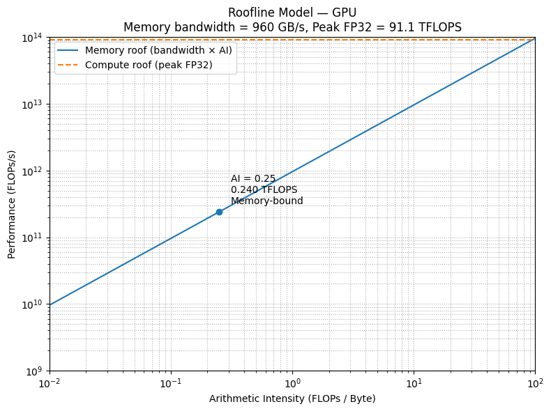
\[\frac{2MNK}{MN(2K + 1) \times 4} \approx 0.25\]Thinking about arithmetic intensity is crucial in deciding whether it’s memory-bound or compute-bound. Let’s check the roofline model:
Roofline model simply states that \(\text{Attainable Performance} = \min(\text{Peak Performance}, \text{AI} \times \text{Peak Bandwidth})\)
With AI (FLOPs/Byte) being the x-axis, Attainable Performance (FLOPs/s) being the y-axis, the graph is first linear then flat, meaning performance first scales with AI, until capped by peak performance. Check out this blog which provides a dynamic plot
Part 3: Shared Memory Tiling (v1)
One can also think about sgemm_v0 from another perspective, each row of A is loaded multiple times (N times to be specific), which is a huge waste, because many threads could have re-used loaded data. For example, thread t0 which is responsible for calculating C(0, 0) and thread t1 which is responsible for calculating C(0, 1), both load A[0][:]
On one end, if we can load the entire matrix to shared memory of a block (TILE_SIZE = Order), then we don’t need to load elements for even a second time. On the other end, if TILE_SIZE = 1, this falls back to sgemm_v0.
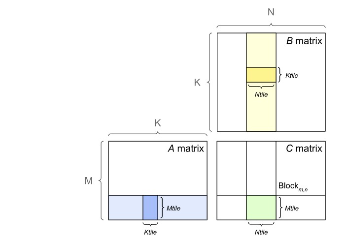 Image Source: Matrix Multiplication Background User’s Guide
Instead of loading vecA(1, K) and vecB(K, 1) into per-thread register space, here we are loading vecA(TILE_SIZE, K) and vecB(K, TILE_SIZE) into per-block shared memory. Since these sizes are too large, we break them into tiles and accumulate them by phases.
float sum = 0.0f;

for (int ph = 0; ph < CEIL(K, BK); ph++) {
    load_as(ph);
    load_bs(ph);
    __syncthreads();
    update_sum();
    __syncthreads();
}

store_c();
Computation of each block computation vecA(TILE_SIZE, K) multiply vecB(K, TILE_SIZE):
Memory accesses of each block:
\[TK + KT + T^2\]Arithmetic intensity:
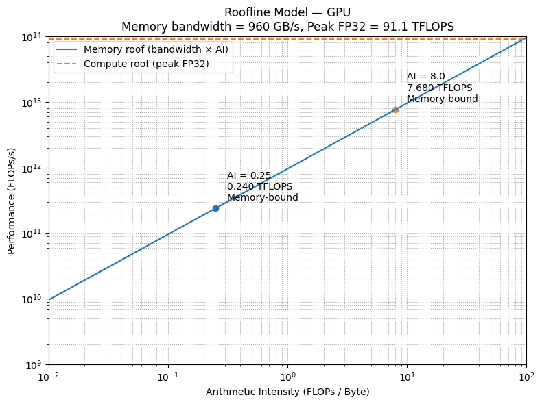
\[\frac{2 T^2K}{(TK + KT + T^2) \times 4} \approx 0.25 T\]With shared memory, arithmetic intensity is amplified by
TILE_SIZEcompared withsgemm_v0because of the reduced global memory access
Assuming a TILE_SIZE = 32:
Part 4: Switching to Outer Product
FMA
FMA = “Fused Multiply-Add Operation”. For operations such as $X \times Y + Z$, instead of first calculating $X\times Y$ and then $+Z$, which is essentially two steps, FMA is able to carry it out with one rounding step.
FMA was added to the IEEE 754 standard in its 2008 revision, and since it has only one rounding step instead of two, it is more accurate.
The nvcc compiler automatically generates FMA instructions for our kernels.
FMA instructions are important when we think about how many FMA instructions we need to overlap memory access latency.
Inner Product V.S. Outer Product
In previous section, we see that one way of doing matrix multiplication is to take dot product (or inner product) of rows in A and cols in B to have a full element in C
Alternatively, one could also use outer product to do matrix multiplication:
for (int k = 0; k < K; k++) {
    for (int m = 0; m < M; m++) {
        for (int n = 0; n < N; n++) {
            C[m][n] += A[m][k] * B[k][n];
        }
    }
}
I view it as, along the inner dimension K, take one column col(M, 1) in A and one row row(1, N) in B, perform outer product, update according entries in C.
- Both methods have the same amount of computations (FLOPs), which is $2MNK$ (or $MNK$ FMAs), but they have quite different memory access patterns.
Not considering (Even considering) shared memory, inner products require each row of A and column of B to be loaded multiple times, while doing outer product requires each A col and B row to be loaded only once.
- Namely for the same amount of memory loaded, they have different AI
Consider doing one A row ($1\times 4$) inner product one B col ($4 \times 1$), it produced 4 FMA instructions
However for one A col and one B row, it produced 16 FMA instructions
- The problem for outer product is that, each time it will write into a large array that might be beyond its cache capacity, but inner product will only write into one element.
Instead of calculating and writing into a big $C$ array, we will stick to our previous framework, cutting $A$ and $B$ into small tiles, and “accumulate” these results before writing it back to global memory.
Thread Tile (v2)
Since we are doing outer product now, each thread will need to calculate not just one, but a block of elements, denoted by $TM \times TN$. Each time we accumulate along the $K$ dimension, this matrix of elements gets updated.
Namely, for each thread, to get a product of $TM \times TN$, we are doing matmul of $TM \times K$ and $K \times TN$. Since K is too large, we still accumulate them by phases. In each phase, each thread first load elements from global memory to shared memory, and then from shared memory to registers.
for (int ph = 0; ph < CEIL(K, BK); ph++) {
    load_as(ph);
    load_bs(ph);
    __syncthreads();
    for (int k = 0; k < BK; k++) {
        load_ar(k);
        load_br(k);
        mma();
    }
    __syncthreads();
}
Shared memory tiling is still needed because multiple threads (from different warps) might access the same rows and cols. Let’s revisit the AI (for each tile, still only considering global memory access):
\[\text{AI} = \frac{2 \times BM \times BN \times BK}{4\times(BM \times BK + BK \times BN)} = \frac{1}{2(\frac{1}{BM} + \frac{1}{BN})}\]- With larger $BM$ and $BN$, comes larger AI
- AI is maximized when $BM = BN$
Here I picked $BM = BN = 128, BK = 8$, $TM = TN = 8$ (so there are $\frac{BN}{TN}\times \frac{BM}{TM} = 256$ threads per block)
Part 5: Reduced bank conflict (v3)
Bank conflict, in my understanding, happens when multiple threads within the same warp try to access different memory locations of the same memory bank of shared memory.
Previously in sgemm_v1, we do not have any bank conflict:
In
sgemm_v1, sinceTILE_SIZE = 32, which is essentially warp size, all threads in the same warp are accessing the sameAsrow (same element) and differentBscol when doing inner product.Asrow is broadcasted to each thread, while eachBscol falls into different memory bank.
But now we do, because each thread is playing with multiple rows and cols at the same time.
Since we have 16 threads along the x-axis and y-axis, thread 0 and thread 16 are bound to access different rows but the same column at the same time.
This can also be told by looking at
load_arfunction.Ar[i] = As[i + thread_row][k];whereint thread_row = threadIdx.y * TM;So y-axis-neighbouring threads will access element that are $TM \times BK \times 4$ bytes away, while $32 \times 4$ bytes along causes bank conflict.
In this case, I choose to transpose As to solve the problem.
__shared__ float AsT[BK][BM];
auto load_ast = [&](int ph) {
    int nelements = BM * BK;
    for (int i = tid; i < nelements; i += nthreads) {
        int shmem_row = i / BK;
        int shmem_col = i % BK;
        int a_row = block_row + shmem_row;
        int a_col = ph * BK + shmem_col;
        if (a_row < M && a_col < K) {
            AsT[shmem_col][shmem_row] = A[OFFSET(a_row, a_col, M, K)];
        } else {
            AsT[shmem_col][shmem_row] = 0.0f;
        }
    }
};

auto load_ar = [&] (int k) {
    for (int i = 0; i < TM; i++) {
        Ar[i] = AsT[k][i + thread_row];
    }
};
Note that:
- Instead of loading
A[a_col][a_row]intoAsT[sh_row][sh_col] - I load
A[a_row][a_col]toAsT[sh_col][sh_row]
Because I want to keep global memory access to stay coalesced.
Part 6: Vectorized load (v4)
CUDA also provides SIMD-like semantics, enabling each thread to load 4 floats instead of just 1 at a time from memory (global memory/shared memory).
#define FLOAT4(pointer)	(reinterpret_cast<float4*>(&(pointer))[0])
/* Load B[global_idx : global_idx + 4] to Bs[shmem_row][shmem_col : shmem_col + 4] */
FLOAT4(Bs[shmem_row][shmem_col]) = FLOAT4(B[global_idx]);
The loading logic (global memory to shared memory, shared memory to register):
auto load_bs = [&](int ph) {
    int nelements = BK * BN;
    for (int i = 4 * tid; i < nelements; i += 4 * nthreads) {
        int shmem_row = i / BN;
        int shmem_col = i % BN;
        int b_row = ph * BK + shmem_row;
        int b_col = block_col + shmem_col;
        if (b_row < K && b_col < N) {
            FLOAT4(Bs[shmem_row][shmem_col]) = FLOAT4(B[OFFSET(b_row, b_col, K, N)]);
        } else {
            FLOAT4(Bs[shmem_row][shmem_col]) = make_float4(0.f,0.f,0.f,0.f);
        }
    }
};

auto load_br = [&] (int k) {
    for (int i = 0; i < TN; i += 4) {
        FLOAT4(Br[i]) = FLOAT4(Bs[k][i + thread_col]);
    }
};
The caveat is you have to load the 4 floats from an address of a multiple of 16 and not just 4, namely you cannot just load ANY consecutive 4 floats.
For example, if you are dealing with matrix multiplication of two
15 × 15matrices withTILE_SIZE = 4, a total of4 × 4tiles are needed, andTILE(1, 0)essentially loadMat[4:8][0:4]to shared memory
It is natural to think, why not simply use 4 float4 to load elements from global memory to 4 × 4 shared memory tile?
Mat[4][0] = Mat[60]would be legal forfloat4operation, whileMat[5][0] = Mat[75]is NOT
Previously, I did a lot of branching in one kernel to decide if a location is suitable for float4 (for irregular matrices), but then I discovered that the benefit of using float4 in these scenarios are too marginal to cover the cost of divergence of threads.
Therefore, I directly fall back to the non-float4 version (which is sgemm_v3) when facing irregular matrices, and only use float4 for those that are a fit.
Part 7: Occupancy Analysis
Computation is so much faster than memory accesses in GPU (and also CPU), so when a warp is waiting for data movement from global memory to register, or even shared memory to register, the SM’s warp scheduler (an Ada SM has four) will pick the next runnable warp, instead of stalling and waiting for the data.
If there is no runnable warp, then the scheduler has no choice but to wait, and our computation unit is stalling, computation power wasted.
This is where the concept of occupancy kicks in.
Occupancy is defined as the ratio of active warps on an SM to the maximum number of active warps supported by the SM.
One key factor that decides occupancy is resource constraints, such as registers per thread, shared memory per block and the maximum number of concurrent warps.
Higher occupancy is not always better, because we have more warps to hide memory access latencies, but a too low occupancy is definitely not optimal!
For my environment setup:
- Each block uses $(BM \times BK + BK \times BN) \times 4 = 8192 = 8\text{KB}$ Shared Memory, plus $1\text{KB}$ for CUDA runtime overhead
- Each block needs at least $(TM \times TN + TM + TN) \times \frac{BN}{TN} \times \frac{BM}{TM} = 20480$ Registers, for the accumulators and fragments alone
From these calculations alone, the block limit by shared memory would be $5$ (assuming 48 KB of shared memory per SM) and the block limit by registers would be $3$. Both estimates are off, so we should check with the Nsight Compute profiler:
Section: Occupancy
------------------------------- ----------- ------------
Metric Name                     Metric Unit Metric Value
------------------------------- ----------- ------------
Block Limit SM                        block           24
Block Limit Registers                 block            2
Block Limit Shared Mem                block            7
Block Limit Warps                     block            6
Theoretical Active Warps per SM        warp           16
Theoretical Occupancy                     %        33.33
Achieved Occupancy                        %        30.91
Achieved Active Warps Per SM           warp        14.84
------------------------------- ----------- ------------
The profiler’s block limits differ from my estimates for two reasons:
- Registers: the compiler also needs registers for indices, addresses and loop counters. Nsight Compute reports 127 registers per thread for
sgemm_v4, which the hardware allocates as 128, so a block of 256 threads needs $128 \times 256 = 32768$ registers and only $65536 / 32768 = 2$ blocks fit. - Shared memory: an Ada SM has 128 KB of on-chip memory shared between the L1 cache and shared memory (at most 100 KB of shared memory), and the driver picks the split (the carveout). Here it chose 64 KB of shared memory, so $\lfloor 64 / 9 \rfloor = 7$ blocks fit.
Note that the above table makes sense because
\[\text{\#warps per block} =\frac{\frac{BN}{TN} \times \frac{BM}{TM}}{\text{Warp Size}} = \frac{16\times16}{32} = 8\] \[\text{\#blocks per SM} = 2\] \[\text{\#warps per SM} = 8 \times 2 = 16\] \[\text{Occupancy} = \frac{\text{\#warps per SM}}{\text{\#Max Warps per SM}} = \frac{16}{48} = \frac{1}{3} \approx 33.333\%\]Our kernel is very balanced, and occupancy looks fine!
Additionally Required
In the original school project, we are also required:
- Find not just one but two minimums of the product
Cand their 2D indices - Parallelize as much as possible! (No sequential reduction in the main process)
- Perform SSSP algorithm on these two minimums